Label
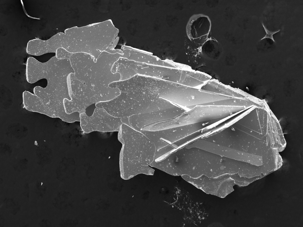
SEM Imaging of Polycrystalline Samples of Cr Intercalated TaTe2
Artist
David Saakov
Description
This image was created using the JOEL Scanning Electron Microscope in the Chemical Sciences Laboratory using 25kV accelerating voltage for higher resolution. The SEM is a high-powered microscope using electron beams to capture images of extremely small samples, in this case, a polycrystalline sample of Cr intercalated TaTe2. Furthermore, the SEM on campus is also attached with an EDS which can elementally map and point ID a sample to show the composition of the elements and confirm the elements present in a sample.
Here you can see how these crystals grow in thin sheets, which is very common in these types of 2-D materials. These materials are very commonly used in many wide applications involving energy storage, electronics and optoelectronics, quantum computing, sensors, magnetic materials, etc.
Type
Scanning Electron Microscope
Artist Affiliation
Graduate Student
Department
Department of Chemistry and Biochemistry
Area of Research
Solid State Chemistry and Magnetism
Research Group Site
Date
2025